[Next]
[Previous] [Up] [Top] [Contents] [Back]Chapter 4 Theory of Operation
The board is divided into four channels, each consisting of eight inputs. Each individual input consist of:
| a current limiting resistor (R4-R35), | |
| a bias resistor (R36-R67), | |
| a reverse current protection diode (D1-D32),
| |
| an opto-coupler IC (U1-U32), | |
| a pull-up resistor (RN4-RN7) and | |
| a debounce circuit (U34, U36, U38, U40, U43
and U45). |
The current limiting and the bias resistors determine the "on" and "off" input current values.
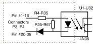
Figure 4-1 Input Network
The debounce circuit has a programmable debounce time which is set by the value of C2 following the equation:
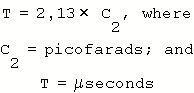
The debounce IC U40 is used to generate the debounce clock. This clock is fed to the other debounce IC's U34, U36, U38, U43 and U45 through U47. U47 is used as a non-inverting buffer. Data from the debouncers have an inverted polarity.
![]()
[Next]
[Previous] [Up] [Top] [Contents] [Back]
![]()